
|
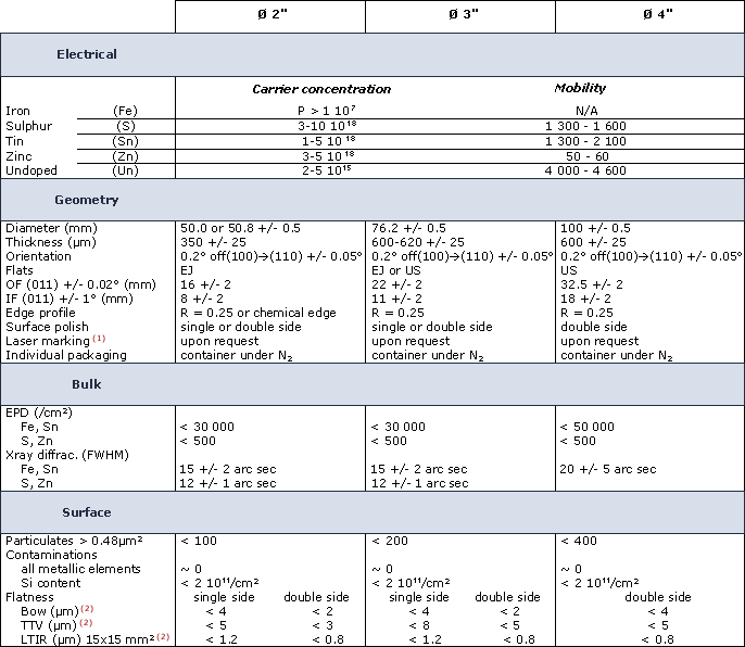
|||||||
|
|
|
| InPACT keeps in inventory a three-month supply of as-sliced wafers in most categories of the standard product lines but ... | |
 |
|
| - off orientation wafers (2° off, (311), (111)A or B
.),
- Rectangular wafers (25 x 30mm), - Test grade wafers Most of our production is made up of premium grade wafers. However, in every boule, some test grade wafers are available. Test wafers have the same electrical performance and geometrical specification than premium wafers but with a small local damage : - a surface defect like a scratch or a pit or a stain on the front side, - a crystalline imperfection like high EPD or a twin lamellae. The latter is made up of 2 parallel lines in the <110> direction. Between these 2 lines, the orientation is not (100) contrary to the whole wafer ; the distance between the 2 lines is very small (< 1mm). Over 95 % of the whole surface is premium quality which makes them useful for calibration runs. The type of defect is indicated on a label for each wafer. |
|