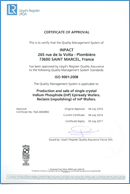
 Download our
certificate of approval
ISO 9001
|
 |
 |
 |
- The largest Western producer of Indium Phosphide substrates covering all dopants (Fe, Sn, Zn, S) and all diameters (2", 3", 4").
- Dedicated exclusively to InP, InPACT provides high-performance substrates for a wide range of devices primarily for optoelectronic applications for fiber optics telecoms and datacoms (for LED, LD, PIN, APD, SOA type of chips).
- Founded in 1995, InPACT has an extensive manufacturing experience (30 years) of InP.
- InPACT is an independent, private company owned by two founders/shareholders (AlmaphotonX, France and Betatech, China) .
- The plant is located in the French Alps, near the high tech Center of Grenoble. With the current design and on-going expansion plan, it enables to increase gradually production capacity x 6 within the next 12 months.
- InPACT serves 60+ customers worldwide (Europe, China, Japan, US). The customer profile includes leading telecom/ datacom epitaxy related and components producers, start-ups as well as leading Government Research Centers and Universities.
- With its proprietary Epiready technology (EPICLEAN
 ) and its advanced wafering technologies (especially for flatness and contamination level), the company is strategically positioned to be a dominant supplier of InP substrates. ) and its advanced wafering technologies (especially for flatness and contamination level), the company is strategically positioned to be a dominant supplier of InP substrates.
|
|

 Download our
 Download our